USE DISCOUNT CODEEXPERT30TO SAVE $30 USD
Thermal Pad/Vias
JSCBLOG , 01-17-2020, 01:03 AM
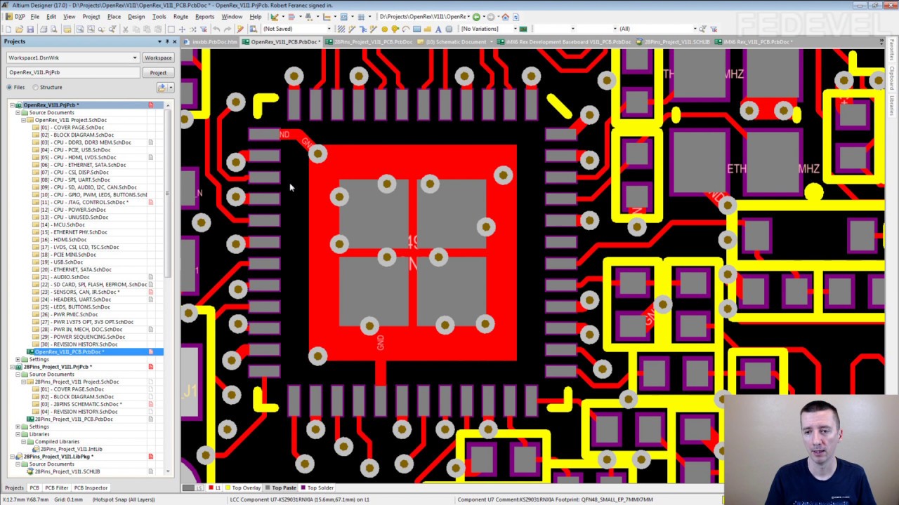
Hey, I'm using a chip (BQ24092DGQR) with a thermal pad underneath. How will I go about designing it? Do I just have a large area underneath it with just top paste layer, for creating the thermal pad? Also the datasheet mentions thermal vias...are they just normal vias in Altium? I put the datasheet below:
There's a video awhile back, is this related to my question?

There's a video awhile back, is this related to my question?
Lakshmi , 01-17-2020, 05:35 AM
Yes, You need to connect the Thermal pad to the VSS(GND)using via.
Yes Robert's video is related to that.
You can also have a look at the Evaluation board Layout (http://www.ti.com/product/BQ24092/toolssoftware) and also look at the 12. Layout section of the data sheet(Page No 28)
Thank you.
Yes Robert's video is related to that.
You can also have a look at the Evaluation board Layout (http://www.ti.com/product/BQ24092/toolssoftware) and also look at the 12. Layout section of the data sheet(Page No 28)
Thank you.
robertferanec , 01-20-2020, 01:36 AM
- I would follow footprint and paste recommendations from the datasheet you attached
- I am speaking about exposed pad and footprints in this video: https://www.youtube.com/watch?v=cMxXea16Hxc
- I am speaking about exposed pad and footprints in this video: https://www.youtube.com/watch?v=cMxXea16Hxc
Use our interactive Discord forum to reply or ask new questions.